Radio frequency (RF) refers to the rate of oscillation of electromagnetic radio waves in the range of 3 kHz to 300 GHz, as well as the alternating currents carrying the radio signals. This is the frequency band that is used for communications transmission and broadcasting.
Radio frequency is produced by oscillating current a specified number of times and then radiating it off a conductor, referred to as an antenna, into empty space (this refers to space occupied by air rather than solid objects and does not refer to outer space) as electromagnetic radio waves. RF signals are sent and received using conductors through the phenomenon known as the skin effect, where RF current latches itself and flows through the surface of conductors rather than penetrating and passing through them like it does with other non-conducting solids. This effect is the core and basis of radio technology.Radio frequency (RF) refers to the rate of oscillation of electromagnetic radio waves in the range of 3 kHz to 300 GHz, as well as the alternating currents carrying the radio signals. This is the frequency band that is used for communications transmission and broadcasting.
Today we are going to build a simple one way wireless communication using RF. It will be suitable for short distances as the frequency of transmission we are choosing is 433 MHz. We could have used IR(Infra Red) Waves also for short distances but it requires line of sight so we are preferring RF Waves.
Here we are using a very basic circuit to demonstrate the working of RF transmitter and receiver.
Materials Used
433 MHz RF Transmitter and Receiver
HT12D Decoder IC
HT12E Encoder IC
Push Buttons (3 Nos)
LEDs (3 Nos)
1M ohm, 47K ohm
7805 Voltage Regulator
9V Battery (2Nos)
The transmitter module has three pins Vcc, Din and GND. The Vcc pin has range of input from 6V to 12V DC usually. So we can give this power using a battery of 9V or adapters of output in this range. Signal Data is fed through the Din pin. GND is connected to the ground. This signal is then modulated using the ASK (Amplitude Shift Keying) and then sent on air at a frequency of 433MHz. The speed at which it can transmit data is around 10Kbps.
The reciever module has 4 pins namely, Vcc , Dout, Linear out, and ground as shown below. The two pins Din and Serial out are shorted together.

A simple one way communication can be done by using transmitters and receivers only. If Din is made high on transmitter side, we will get Dout pin high on the receiver side. But this method has some serious draw backs as this can be utilized only for single signal and also data is not encrypted and there are chances interference with other modules nearby.
To solve this problem we use encoders and decoders. The HT12D and HT12E are 4-data bit encoder and decoder modules. So there can be (2^4 = 16) 16 different combinations of inputs and outputs. There are 18 pin IC’s which can operate between 3V to 12V input power supply. They have 4-data bit and 8-address bit, these 8 address bits has to be set same on both the encoder and decoder to make them work as a pair. This makes sure that data transmission is done between same a pair of encoder and decoder.Also by using these address pins we can provide 8 bit security code for data transmission and multiple receivers may be addressed using the same transmitter.
Pin Out OF HT12E (Encoder)
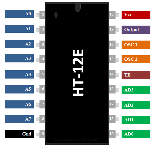
Pin 1-8: Input pins for address A0~A7. These pins can be externally set to VSS(GND) or left open but the configuration has to be same on decoder side as well HT-12 D
Pin 9: Denoted as VSS is connected to the GND
NOTE: VCC (Voltage Common Collector) is the higher voltage with respect to GND (ground). VSS can be negative or ground but when only positive power supply is used then VSS (Voltage Source Supply) is connected to ground everywhere.
Pin 10-13. AD in this pins is for to transmitting data of 4 bits. These are active low pins that means to make any pin active it has to be connected to Vss or it can be left open for inactive state.
Pin 14. Transmission enable, it can be done connecting this pin to GND. The transmission occurs only when this pin is connected to ground.
Pin 15 and 16: OSC1 and OSC2 are used to connect external resistance for the internal oscillator. OSC1 is the oscillator input pin and OSC2 is the oscillator output pin. Here 1 MOhm resistor is to be connected . This resistance is determined by the datasheet supplied by manufacturer. 1 Mohm works fine for most of the HT12E ICs.
Pin 17 : It is the serial data output of the encoder and can be connected to a RF transmitter.
Pin 18: This pin VCC is connected to the positive trminal of our supply.
PINOUT OF HT12D (DECODER)
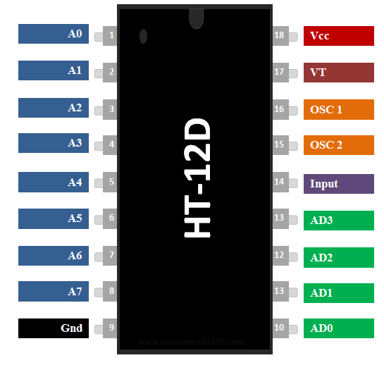
Pin 1-8. These pins can be connected to ground or left open but the configuration has to match excatly to that of HT12E for communication.
Pin 9. VSS this pin is connected to GND.
Pin 10-13. “AD0-AD3” : Output data pins, power-on state is low. The output is same which was send from the transmitter. This means we will get the same high low combination as in the encoder side.
Pin 14. “DIN” Serial data input pin . This pin is connected to the DATA of our 433 Mhz RF receiver. That means receiver receives the encoded data from transmitter and this data is sent to decoder through DIN pin.
Pin 15-16. In this port a resistor with a value of 51 k ohms or very very close value like 50 k or 52 k is connected.
Pin 17. No connections needed. This pin is automatically if there is valid transmission.
Pin 18. This pin is connected to VCC or the positive of our power source.
Circuit Diagram of RF Transmitter and Receiver:
After understanding the pins circuit can be easily made with the help of circuit diagrams provided below.

